Our NanoNews Digest Sponsors
Home > Press > Stress-free path to stress-free metallic films paves the way for next-gen circuitry: Optimized sputtering technique helps minimize stress in tungsten thin films
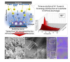
(top left) An illustration of the HiPIMS process (top right) The energy distribution of tungsten ions arriving at the substrate over time. At short times, there are a large proportion of ions with high energy. (bottom) Stress-free tungsten films created with the selective pulsed bias technique. (a) Plan view transmission electron microscopy (TEM) image of the film; (b) a higher resolution image; (c) reconstructions of the selected area in (b) based on inverse Fourier transforms, with two regions magnified.
Related Keywords
Sweden , Japan , Tokyo , Totsukawa , Japan General , Swedish , Tetsuhide Shimizu , Research Awards Scholarships Gifts Contests Honors Records , Tokyo Metropolitan University , Swedish Research Council No , Society International Research Congress , University Faculty Grant , Japan Society For The Promotion Of Science , Wave Inc , Home Press , Chip Technology , Tokyo Metropolitan , Associate Professor Tetsuhide Shimizu , Joint International Research , Japan Society , Swedish Research Council , Swedish Government Strategic Research Area , Materials Science , Functional Materials , Faculty Grant , Nanotechnology Now , Presents Preclinical Data , International Research Congress June , ஸ்வீடந் , ஜப்பான் , டோக்கியோ , ஸ்விட்ச் , ஆராய்ச்சி விருதுகள் உதவித்தொகை பரிசுகள் போட்டிகள் மரியாதை பதிவுகள் , டோக்கியோ பெருநகர பல்கலைக்கழகம் , ஜப்பான் சமூகம் க்கு தி ப்ரமோஶந் ஆஃப் அறிவியல் , அலை இன்க் , வீடு ப்ரெஸ் , சிப் தொழில்நுட்பம் , டோக்கியோ பெருநகர , கூட்டு சர்வதேச ஆராய்ச்சி , ஜப்பான் சமூகம் , ஸ்விட்ச் ஆராய்ச்சி சபை , ஸ்விட்ச் அரசு மூலோபாய ஆராய்ச்சி பரப்பளவு , பொருட்கள் அறிவியல் , செயல்பாட்டு பொருட்கள் , ஆசிரிய மானியம் , நானோ தொழில்நுட்பம் இப்போது ,
comparemela.com © 2020. All Rights Reserved.